Comparing SEM & TEM – Understanding the Pros and Cons

While Scanning Electron Microscopy (SEM) and Transmission Electron Microscopy (TEM) both encompass means of electron imagery, there are some key differences between the two. Firstly, the detailed, three-dimensional and topographical imaging, and the versatile information this provides, is a big reason why SEM is so effective. On the other hand, TEM uses energetic electrons to provide morphologic, compositional and crystallographic two-dimensional information on samples.
In this article, we look at SEM imagery and its wide array of uses, as compared to another means of imaging, TEM.
What is SEM Imagery
SEM scans a focused electron beam over a surface to create an image that can be used to obtain information about the surface topography and composition. It works to produce images by scanning the sample with a high energy beam of electrons. As the electrons interact with the sample, they then produce secondary electrons, backscattered electrons and characteristic X-rays.
What are the Benefits and Disadvantages of SEM
There are a range of benefits associated with using SEM. However, depending on the information required or the type of sample, there are some disadvantages to this method of imaging as well. Before deciding on SEM, the sample type and information required should be the top consideration.
Pros
The power of SEM cannot be underestimated. The process by which the focused beam of electrons creates a magnified image is so advanced that the magnification is anywhere between 10 and 1,000,000 times. As such, it is a key tool for basic research, as well as quality control and failure analysis.
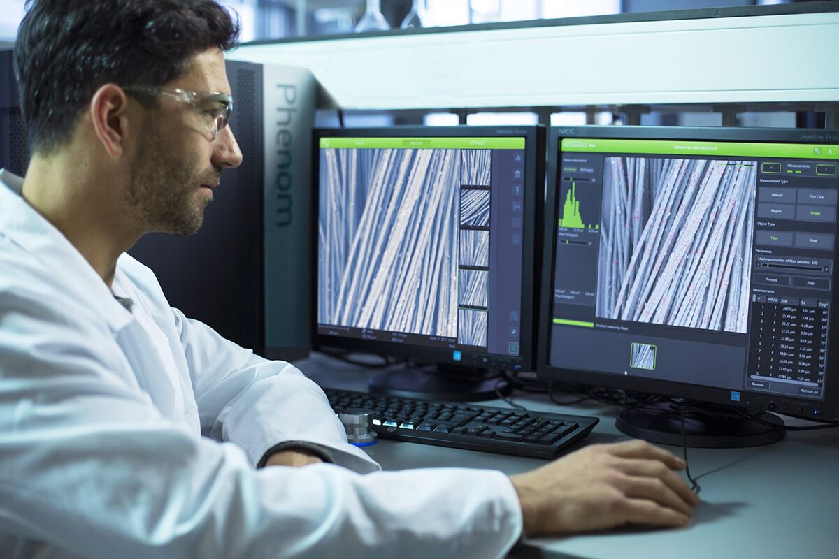
The Phenom Pharos Desktop Scanning Electron Microscope is an affordable desktop SEM that uses a Field Emission Gun (FEG) source commonly only found in larger, more expensive SEM systems housed in Microscopy centers in major Universities. Designed for ease of use, the Phenom Pharos is superfast, enabling imaging in less than 30 seconds after sample loading, and it delivers crisp, high resolution imaging (<3nm) with elemental analysis.
SEM allows for the examination of samples such as metals, alloys and ceramics, as well as polymers and biological materials. It’s practical for sample imaging needed for forensic investigations, biological sciences, soil and rock sampling, and medical science.
In short, if the aim of sample imaging is to examine a relatively large area for surface details and composition, SEM is ideal.
Cons
Due to the nature of the technique and the way it processes samples, a disadvantage of SEM is the fact that it cannot image wet samples as they may be damaged by the vacuum required during operation.
An SEM is also limited when used to image non-conductive samples and colour images, or when used to take measurements involving height. Coating your sample (sputter coating) with an additional thin layer (~10 nm) of a conductive material, such as gold, silver, platinum or chromium, can help remove charging effects and produce better quality images. However, the drawback of sputter coating is it removes the atomic number-contrast and elemental composition analysis.
What is TEM Imagery
TEM is a very powerful tool for material science. A high energy beam of electrons is shone through a very thin sample where the interactions between the electrons and the atoms can be observed. Additionally, chemical analysis can also be performed. The high resolution allows for the analysis of quality, shape and size as well as density.
TEM uses electrons instead of light to reveal the finest details of internal structures, even down to individual atoms.
What are the Benefits and Disadvantages of TEM
TEM offers the most powerful magnification and as such has a wide range of applications that all help to provide information on both element and compound structure. However, despite the advantages of magnification and versatility, there are some disadvantages that need to be taken into account.
Pros
TEM offers powerful magnification with the potential of over one million times, or more. As such, this type of detailed imaging is useful for a variety of fields, from science, to education and industrial uses. The highly detailed images provide valuable insight into elemental and compound structure, lending to providing information on surface features, shape, size and structure.
In short, TEM offers valuable information on the inner structure of the sample, so it’s ideal for individuals looking to gain information pertaining to internal structure.
Cons
TEM is a very large and quite expensive piece of electron microscopy machinery. Due to the complexity of the item, special training is required not only to operate the product, but also to be able to accurately analyse the data that the sample imaging provides.
Moving aside from operating the product, there’s some laborious work involved in preparing a sample for analysis. Firstly, the nature of the sample needs to be taken into consideration. Specifically, will the sample be able to withstand the vacuum chamber? The sample needs to be sliced thin enough for electrons to pass through, but also be able to withstand the process of analysis.
Additionally, sample analysis is limited to materials that are electron transparent.
Let ATA Scientific Find Your Next SEM Solution
When it comes to choosing between SEM and TEM, one technique isn’t better than the other – it comes down to the analysis required. Looking for internal details of small samples, TEM is useful. Need to determine surface information, SEM is best. For more information regarding Scanning Electron Microscopes and Transmission Electron Microscopy contact us today at ATA Scientific.


 02 9541 3500